
Part Datasheet Search > Development Kits > TI > DAC34SH84EVM Datasheet PDF > DAC34SH84EVM Datasheet Pages 1/85
DAC34SH84EVM Datasheet - TI
| Manufacturer: | TI |
| Category: | Development Kits |
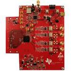
| Description: | Evaluation Module, Digital to Analog Converter, 16Bit, 1.5GSPS, DAC34SH84 |
| Pictures: |
DAC34SH84EVMDatasheet PDF
Page:
of 85 Go
If the format of the manual is confusing, please download and read the original PDF file.

SerDes
CleanedClock
Data
DSP
CDCE62005
RecoveredClock
DSP Clock
ADCClock
ADCClock
DACClock
Product
Folder
Sample &
Buy
Technical
Documents
Tools &
Software
Support &
Community
Reference
Design
CDCE62005
SCAS862F –NOVEMBER 2008–REVISED JANUARY 2015
CDCE62005 3:5 Clock Generator, Jitter Cleaner with Integrated Dual VCOs
1 Features 3 Description
The CDCE62005 is a high performance clock
1
• Superior Performance:
generator and distributor featuring low output jitter, a
– Low Noise Clock Generator: 550 fs rms typical
high degree of configurability via a SPI interface, and
(10 kHz to 20 MHz Integration Bandwidth),
programmable start up modes determined by on-chip
F
C
= 100 MHz
EEPROM. Specifically tailored for clocking data
converters and high-speed digital signals, the
– Low Noise Jitter Cleaner: 2.6 ps rms typical
CDCE62005 achieves jitter performance well under 1
(10 kHz to 20 MHz Integration Bandwidth),
ps RMS (10 kHz to 20 MHz integration bandwidth).
F
C
= 100 MHz
The CDCE62005 incorporates a synthesizer block
• Flexible Frequency Planning:
with partially integrated loop filter, a clock distribution
– 5 Fully Configurable Outputs: LVPECL, LVDS,
block including programmable output formats, and an
LVCMOS and Special High Swing Output
input block featuring an innovative smart multiplexer.
Modes
The clock distribution block includes five individually
– Unique Dual-VCO Architecture Supports a
programmable outputs that can be configured to
Wide Tuning Range: 1.750 GHz to 2.356 GHz
provide different combinations of output formats
(LVPECL, LVDS, LVCMOS). Each output can also be
– Output Frequency Ranges from 4.25 MHz to
programmed to a unique output frequency (up to 1.5
1.175 GHz in Synthesizer Mode
GHz) and skew relationship via a programmable
– Output Frequency up to 1.5 GHz in Fan-Out
delay block (note that frequency range depends on
Mode
operational mode and output format selected). If all
outputs are configured in single-ended mode (for
– Independent Coarse Skew Control on all
example, LVCMOS), the CDCE62005 supports up to
Outputs
ten outputs. Each output can select one of four clock
• High Flexibility:
sources to condition and distribute including any of
– Integrated EEPROM Determines Device
the three clock inputs or the output of the frequency
Configuration at Power-up
synthesizer. The input block includes two universal
differential inputs which support frequencies in the
– Smart Input Multiplexer Automatically Switches
range of 40 kHz to 500 MHz and an auxiliary input
Between One of Three Reference Inputs
that can be configured to connect to an external
• 7 × 7 mm 48-pin VQFN Package (RGZ)
crystal via an on chip oscillator block.
• –40°C to 85°C Temperature Range
The smart input multiplexer has two modes of
operation, manual and automatic. In manual mode,
2 Applications
the user selects the synthesizer reference via the SPI
• Wireless Infrastructure
interface. In automatic mode, the input multiplexer will
automatically select between the highest priority input
• Switches and Routers
clock available.
• Medical Electronics
• Military and Aerospace
Device Information
(1)
• Industrial
PART NUMBER PACKAGE BODY SIZE (NOM)
CDCE62005 VQFN (48) 7.00 mm × 7.00 mm
(1) For all available packages, see the orderable addendum at
the end of the datasheet.
Application Example
1
An IMPORTANT NOTICE at the end of this data sheet addresses availability, warranty, changes, use in safety-critical applications,
intellectual property matters and other important disclaimers. PRODUCTION DATA.