
Part Datasheet Search > Digital to Analog > TI > DAC34SH84IZAYR Datasheet PDF > DAC34SH84IZAYR Datasheet Pages 1/93
DAC34SH84IZAYR Datasheet - TI
| Manufacturer: | TI |
| Category: | Digital to Analog |
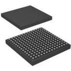
| Case Package: | NFBGA-196 |
| Description: | Quad-Channel, 16Bit, 1.5GSPS, 1x-16x Interpolating Digital-to-Analog Converter (DAC) 196-NFBGA -40℃ to 85℃ |
| Pictures: |
DAC34SH84IZAYRDatasheet PDF
Page:
of 93 Go
If the format of the manual is confusing, please download and read the original PDF file.

DAC34SH84
16-bit DAC
16-bit DAC
16-bit DAC
16-bit DAC
Complex Mixer
(32-bit NCO)
xN
xN
Complex Mixer
(32-bit NCO)
xN
xN
32-Bit LVDS Input Data Bus
RF
RF
LVDS Interface
Product
Folder
Sample &
Buy
Technical
Documents
Tools &
Software
Support &
Community
Reference
Design
DAC34SH84
SLAS808E –FEBRUARY 2012–REVISED SEPTEMBER 2015
DAC34SH84 Quad-Channel, 16-Bit, 1.5 GSPS Digital-to-Analog Converter (DAC)
A high-performance low-jitter clock multiplier
1 Features
simplifies clocking of the device without significant
1
• Low Power: 1.8 W at 1.5 GSPS, Full Operating
impact on the dynamic range. The digital quadrature
Condition
modulator correction (QMC) enables complete IQ
• Multi-DAC Synchronization
compensation for gain, offset and phase between
channels in direct upconversion applications.
• Selectable 2×, 4×, 8×, 16× Interpolation Filter
Digital data is input to the device through a 32-bit
– Stop-Band Attenuation > 90 dBc
wide LVDS data bus with on-chip termination. The
• Flexible On-Chip Complex Mixing
wide bus allows the processing of high-bandwidth
– Two Independent Fine Mixers With 32-Bit
signals. The device includes a FIFO, data pattern
NCOs
checker, and parity test to ease the input interface.
The interface also allows full synchronization of
– Power-Saving Coarse Mixers: ± n × f
S
/ 8
multiple devices.
• High-Performance, Low-Jitter Clock-Multiplying
PLL
The device is characterized for operation over the
entire industrial temperature range of –40°C to 85°C
• Digital I and Q Correction
and is available in a 196-ball, 12-mm × 12-mm, 0.8-
– Gain, Phase and Offset
mm pitch NFBGA package.
• Digital Inverse Sinc Filters
The DAC34SH84 low-power, high-bandwidth support,
• 32-Bit DDR Flexible LVDS Input Data Bus
superior crosstalk, high dynamic range, and features
– 8-Sample Input FIFO
are an ideal fit for next-generation communication
systems.
– Supports Data Rates up to 750 MSPS
– Data Pattern Checker
Device Information
(1)
– Parity Check
PART NUMBER PACKAGE BODY SIZE (NOM)
• Temperature Sensor
DAC34SH84 NFBGA (196) 12.00 mm x 12.00 mm
• Differential Scalable Output: 10 mA to 30 mA
(1) For all available packages, see the orderable addendum at
• 196-Ball, 12-mm × 12-mm NFBGA
the end of the data sheet.
Simplified Schematic
2 Applications
• Cellular Base Stations
• Diversity Transmit
• Wideband Communications
3 Description
The DAC34SH84 is a very low-power, high-dynamic
range, quad-channel, 16-bit digital-to-analog
converter (DAC) with a sample rate as high as
1.5 GSPS.
The device includes features that simplify the design
of complex transmit architectures: 2× to 16× digital
interpolation filters with over 90 dB of stop-band
attenuation simplify the data interface and
reconstruction filters. Independent complex mixers
allow flexible carrier placement.
1
An IMPORTANT NOTICE at the end of this data sheet addresses availability, warranty, changes, use in safety-critical applications,
intellectual property matters and other important disclaimers. PRODUCTION DATA.