Part Datasheet Search > Digital to Analog > TI > DAC34SH84IZAY Datasheet PDF > DAC34SH84IZAY Datasheet Pages 4/93
DAC34SH84IZAY Datasheet - TI
| Manufacturer: | TI |
| Category: | Digital to Analog |
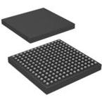
| Case Package: | LFBGA-196 |
| Description: | Quad-Channel, 16Bit, 1.5GSPS, 1x-16x Interpolating Digital-to-Analog Converter (DAC) 196-NFBGA -40℃ to 85℃ |
| Pictures: |
DAC34SH84IZAYDatasheet PDF
Page:
of 93 Go
If the format of the manual is confusing, please download and read the original PDF file.

DAC34SH84
SLAS808E –FEBRUARY 2012–REVISED SEPTEMBER 2015
www.ti.com
Pin Functions
PIN
I/O DESCRIPTION
NAME NO.
D10, E11,
F11, G11,
AVDD I Analog supply voltage. (3.3 V)
H11, J11,
K11, L10
CMOS output for ALARM condition. The ALARM output functionality is defined through the config7
ALARM N12 O register. Default polarity is active-high, but can be changed to active-low via the config0
alarm_out_pol control bit.
Full-scale output current bias. For 30-mA full-scale output current, connect 1.28 kΩ to ground.
BIASJ H12 O
Change the full-scale output current through coarse_dac(3:0) in config3, bit<15:12>.
Internal clock buffer supply voltage. (1.35 V). It is recommended to isolate this supply from DIGVDD
CLKVDD C12, K12 I
and DACVDD.
LVDS positive input data bits 0 through 15 for the AB-channel path. Internal 100-Ω termination
A7, A6, A5,
resistor. Data format relative to DATACLKP/N clock is double data rate (DDR).
A4, A3, A2,
A1, C4, C2,
DAB15P is the most-significant data bit (MSB).
DAB[15..0]P I
D4, D2, E4,
DAB0P is the least-significant data bit (LSB).
E2, F4, F2,
G4
The order of the bus can be reversed via the config2 revbus bit.
B7, B6, B5,
B4, B3, B2,
B1, C3, C1, LVDS negative input data bits 0 through 15 for the AB-channel path. (See the preceding DAB[15:0]P
DAB[15..0]N I
D3, D1, E3, description.)
E1, F3, F1,
G3
H4, J4, J2, LVDS positive input data bits 0 through 15 for the CD-channel path. Internal 100-Ω termination
K4, K2, L4, resistor. Data format relative to DATACLKP/N clock is double data rate (DDR).
L2, M4, M2,
DCD15P is the most-significant data bit (MSB).
DCD[15..0]P I
N1, N2, N3,
DCD0P is the least-significant data bit (LSB).
N4, N5, N6,
The order of the bus can be reversed via the config2 revbus bit.
N7
H3, J3, J1,
K3, K1, L3,
L1, M3, M1, LVDS negative input data bits 0 through 15 for the CD-channel path. (See the preceding DCD[15:0]P
DCD[15..0]N I
P1, P2, P3, description.)
P4, P5, P6,
P7
DACCLKP A12 I Positive external LVPECL clock input for DAC core with a self-bias
DACCLKN A11 I Complementary external LVPECL clock input for DAC core. (See the DACCLKP description.)
D9, E9, E10,
F10, G10, DAC core supply voltage. (1.35 V). It is recommended to isolate this supply from CLKVDD and
DACVDD I
H10, J10, DIGVDD.
K10, K9, L9
LVDS positive input data clock. Internal 100-Ω termination resistor. Input data DAB[15:0]P/N and
DATACLKP G2 I
DCD[15:0]P/N are latched on both edges of DATACLKP/N (double data rate).
DATACLKN G1 I LVDS negative input data clock. (See the DATACLKP description.)
E5, E6, E7,
DIGVDD F5, J5, K5, I Digital supply voltage. (1.3 V). It is recommended to isolate this supply from CLKVDD and DACVDD.
K6, K7
Used as an external reference input when the internal reference is disabled through config27
EXTIO G12 I/O extref_ena = 1. Used as an internal reference output when config27 extref_ena = 0 (default).
Requires a 0.1-μF decoupling capacitor to AGND when used as a reference output.
LVDS input strobe positive input. Internal 100-Ω termination resistor
The main functions of this input are to sync the FIFO pointer, to provide a sync source to the digital
blocks, and/or to act as a parity input for the AB-data bus.
ISTRP/
H2 I
These functions are captured with the rising edge of DATACLKP/N. This signal should be edge-
PARITYABP
aligned with DAB[15:0]P/N and DCD[15:0]P/N.
The PARITY, SYNC, and ISTR inputs are rotated to allow complete reversal of the data interface
when setting the rev_interface bit in register config1.
ISTRN/
H1 I LVDS input strope negative input. (See the ISTRP/PARITYABP description.)
PARITYABN
4 Submit Documentation Feedback Copyright © 2012–2015, Texas Instruments Incorporated
Product Folder Links: DAC34SH84

