Part Datasheet Search > Digital to Analog > TI > DAC34SH84IZAY Datasheet PDF > DAC34SH84IZAY Datasheet Pages 5/93
DAC34SH84IZAY Datasheet - TI
| Manufacturer: | TI |
| Category: | Digital to Analog |
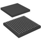
| Case Package: | LFBGA-196 |
| Description: | Quad-Channel, 16Bit, 1.5GSPS, 1x-16x Interpolating Digital-to-Analog Converter (DAC) 196-NFBGA -40℃ to 85℃ |
| Pictures: |
DAC34SH84IZAYDatasheet PDF
Page:
of 93 Go
If the format of the manual is confusing, please download and read the original PDF file.

DAC34SH84
www.ti.com
SLAS808E –FEBRUARY 2012–REVISED SEPTEMBER 2015
Pin Functions (continued)
PIN
I/O DESCRIPTION
NAME NO.
A10, A13,
A14, B10,
B11, B12,
B13, C5, C6,
C7, C8, C9,
C10, C13,
D8, D13,
D14, E8,
E12, E13,
F6, F7, F8,
F9, F12, F13,
G6, G7, G8,
GND G9, G13, I These pins are ground for all supplies.
G14, H6, H7,
H8, H9, H13,
H14, J6, J7,
J8, J9, J12,
J13, K8, K13,
L8, L13, L14,
M5, M6, M7,
M8, M9,
M10, M11,
M12, M13,
N13, P13,
P14
IOUTAP B14 O A-channel DAC current output. Connect directly to ground if unused.
IOUTAN C14 O A-channel DAC complementary current output. Connect directly to ground if unused.
IOUTBP F14 O B-channel DAC current output. Connect directly to ground if unused.
IOUTBN E14 O B-channel DAC complementary current output. Connect directly to ground if unused.
IOUTCP J14 O C-channel DAC current output. Connect directly to ground if unused.
IOUTCN K14 O C-channel DAC complementary current output. Connect directly to ground if unused.
IOUTDP N14 O D-channel DAC current output. Connect directly to ground if unused.
IOUTDN M14 O D-channel DAC complementary current output. Connect directly to ground if unused.
D5, D6, G5,
IOVDD I Supply voltage for all LVDS I/O. (3.3 V)
H5, L5. L6
Supply voltage for all CMOS I/O. (1.8 V to 3.3 V) This supply can range from 1.8 V to 3.3 V to change
IOVDD2 L12 I
the input and output levels of the CMOS I/O.
LPF D12 I/O PLL loop filter connection. If not using the clock-multiplying PLL, the LPF pin can be left unconnected.
Optional LVPECL output strobe positive input. This positive-negative pair is captured with the rising
OSTRP A9 I edge of DACCLKP/N. It is used to sync the divided-down clocks and FIFO output pointer in dual-
sync-sources mode. If unused it can be left unconnected.
OSTRN B9 I Optional LVPECL output strobe negative input. (See the OSTRP description.)
Optional LVDS positive input parity bit for the CD-data bus. The PARITYCDP/N LVDS pair has an
internal 100-Ω termination resistor. If unused, it can be left unconnected.
PARITYCDP N8 I
The PARITY, SYNC, and ISTR inputs are rotated to allow complete reversal of the data interface
when setting the rev_interface bit in register config1.
PARITYCDN P8 I Optional LVDS negative input parity bit for the CD-data bus.
PLLAVDD C11, D11 I PLL analog supply voltage (3.3 V)
SCLK P9 I Serial interface clock. Internal pulldown
SDENB P10 I Active-low serial data enable, always an input to the DAC34SH84. Internal pullup
Serial interface data. Bidirectional in 3-pin mode (default) and unidirectional 4-pin mode. Internal
SDIO P11 I/O
pulldown
Unidirectional serial interface data in 4-pin mode. The SDO pin is in the high-impedance state in 3-pin
SDO P12 O
interface mode (default).
SLEEP N11 I Active-high asynchronous hardware power-down input. Internal pulldown
Copyright © 2012–2015, Texas Instruments Incorporated Submit Documentation Feedback 5
Product Folder Links: DAC34SH84

