
Part Datasheet Search > Digital to Analog > TI > DAC34SH84IZAY Datasheet PDF > DAC34SH84IZAY Datasheet Pages 6/93
DAC34SH84IZAY Datasheet - TI
| Manufacturer: | TI |
| Category: | Digital to Analog |
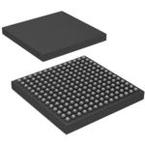
| Case Package: | LFBGA-196 |
| Description: | Quad-Channel, 16Bit, 1.5GSPS, 1x-16x Interpolating Digital-to-Analog Converter (DAC) 196-NFBGA -40℃ to 85℃ |
| Pictures: |
DAC34SH84IZAYDatasheet PDF
Page:
of 93 Go
If the format of the manual is confusing, please download and read the original PDF file.

DAC34SH84
SLAS808E –FEBRUARY 2012–REVISED SEPTEMBER 2015
www.ti.com
Pin Functions (continued)
PIN
I/O DESCRIPTION
NAME NO.
LVDS SYNC positive input. Internal 100-Ω termination resistor. If unused it can be left unconnected.
SYNCP A8 I The PARITY, SYNC, and ISTR inputs are rotated to allow complete reversal of the data interface
when setting the rev_interface bit in register config1.
SYNCN B8 I LVDS SYNC negative input
RESETB N10 I Active-low input for chip RESET. Internal pullup
Transmit enable active-high input. Internal pulldown
To enable analog output data transmission, set sif_txenable in register config3 to 1 or pull the CMOS
TXENA N9 I TXENA pin to high.
To disable analog output, set sif_txenable to 0 and pull the CMOS TXENA pin to low. The DAC
output is forced to midscale.
TESTMODE L11 I This pin is used for factory testing. Internal pulldown. Leave unconnected for normal operation
Digital supply voltage. This supply pin is also used for factory fuse programming. Connect to
VFUSE D7, L7 I
DACVDD or DIGVDD for normal operation
6 Specifications
6.1 Absolute Maximum Ratings
over operating free-air temperature range (unless otherwise noted)
(1)
MIN MAX UNIT
DACVDD, DIGVDD, CLKVDD –0.5 1.5 V
VFUSE –0.5 1.5 V
Supply voltage
range
(2)
IOVDD, IOVDD2 –0.5 4 V
AVDD, PLLAVDD –0.5 4 V
DAB[15..0]P/N, DCD[15..0]P/N, DATACLKP/N, ISTRP/N, PARITYCDP/N,
–0.5 IOVDD + 0.5 V
SYNCP/N
DACCLKP/N, OSTRP/N –0.5 CLKVDD + 0.5 V
ALARM, SDO, SDIO, SCLK, SDENB, SLEEP, RESETB, TESTMODE,
–0.5 IOVDD2 + 0.5 V
Pin voltage range
(2)
TXENA
IOUTAP/N, IOUTBP/N, IOUTCP/N, IOUTDP/N –1.0 AVDD + 0.5 V
EXTIO, BIASJ –0.5 AVDD + 0.5 V
LPF –0.5 PLLAVDD + 0.5 V
Peak input current (any input) 20 mA
Peak total input current (all inputs) –30 mA
Absolute maximum junction temperature, T
J
150 °C
Storage temperature range, T
stg
–65 150 °C
(1) Stresses beyond those listed under Absolute Maximum Ratings may cause permanent damage to the device. These are stress ratings
only, and functional operation of these or any other conditions beyond those indicated under Recommended Operating Conditions is not
implied. Exposure to absolute-maximum-rated conditions for extended periods may affect device reliability.
(2) Measured with respect to GND
6.2 ESD Ratings
VALUE UNIT
Human-body model (HBM), per ANSI/ESDA/JEDEC JS-001
(1)
±2000
V
(ESD)
Electrostatic discharge V
Charged-device model (CDM), per JEDEC specification JESD22-
±500
C101
(2)
(1) JEDEC document JEP155 states that 500-V HBM allows safe manufacturing with a standard ESD control process.
(2) JEDEC document JEP157 states that 250-V CDM allows safe manufacturing with a standard ESD control process.
6 Submit Documentation Feedback Copyright © 2012–2015, Texas Instruments Incorporated
Product Folder Links: DAC34SH84