
Part Datasheet Search > BJTs > ON Semiconductor > MJL21194 Datasheet PDF > MJL21194 Datasheet Pages 1/6
MJL21194 Datasheet - ON Semiconductor
| Manufacturer: | ON Semiconductor |
| Category: | BJTs |
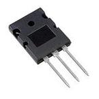
| Case Package: | TO-264-3 |
| Description: | TO-3BPL NPN 250V 16A |
| Pictures: |
MJL21194Datasheet PDF
Page:
of 6 Go
If the format of the manual is confusing, please download and read the original PDF file.

© Semiconductor Components Industries, LLC, 2007
January, 2007 − Rev. 5
1 Publication Order Number:
MJL21193/D
MJL21193, MJL21194
Preferred Device
Silicon Power Transistors
The MJL21193 and MJL21194 utilize Perforated Emitter
technology and are specifically designed for high power audio output,
disk head positioners and linear applications.
Features
• Total Harmonic Distortion Characterized
• High DC Current Gain −
h
FE
= 25 Min @ I
C
= 8 Adc
• Excellent Gain Linearity
• High SOA: 2.25 A, 80 V, 1 Second
• Pb−Free Packages are Available*
ÎÎÎÎÎÎÎÎÎÎÎÎÎÎÎÎÎÎÎ
ÎÎÎÎÎÎÎÎÎÎÎÎÎÎÎÎÎÎÎ
MAXIMUM RATINGS
ÎÎÎÎÎÎÎÎÎÎÎÎ
Rating
ÎÎÎ
Symbol
ÎÎÎÎ
Value
ÎÎÎ
Unit
ÎÎÎÎÎÎÎÎÎÎÎÎ
ÎÎÎÎÎÎÎÎÎÎÎÎ
Collector−Emitter Voltage
ÎÎÎ
ÎÎÎ
V
CEO
ÎÎÎÎ
ÎÎÎÎ
250
ÎÎÎ
ÎÎÎ
Vdc
ÎÎÎÎÎÎÎÎÎÎÎÎ
ÎÎÎÎÎÎÎÎÎÎÎÎ
Collector−Base Voltage
ÎÎÎ
ÎÎÎ
V
CBO
ÎÎÎÎ
ÎÎÎÎ
400
ÎÎÎ
ÎÎÎ
Vdc
ÎÎÎÎÎÎÎÎÎÎÎÎ
ÎÎÎÎÎÎÎÎÎÎÎÎ
Emitter−Base Voltage
ÎÎÎ
ÎÎÎ
V
EBO
ÎÎÎÎ
ÎÎÎÎ
5
ÎÎÎ
ÎÎÎ
Vdc
ÎÎÎÎÎÎÎÎÎÎÎÎ
ÎÎÎÎÎÎÎÎÎÎÎÎ
Collector−Emitter Voltage − 1.5 V
ÎÎÎ
ÎÎÎ
V
CEX
ÎÎÎÎ
ÎÎÎÎ
400
ÎÎÎ
ÎÎÎ
Vdc
ÎÎÎÎÎÎÎÎÎÎÎÎ
Î
ÎÎÎÎÎÎÎÎÎÎ
Î
ÎÎÎÎÎÎÎÎÎÎÎÎ
Collector Current − Continuous
Peak (Note 1)
ÎÎÎ
Î
Î
Î
ÎÎÎ
I
C
ÎÎÎÎ
Î
ÎÎ
Î
ÎÎÎÎ
16
30
ÎÎÎ
Î
Î
Î
ÎÎÎ
Adc
ÎÎÎÎÎÎÎÎÎÎÎÎ
Base Current − Continuous
ÎÎÎ
I
B
ÎÎÎÎ
5
ÎÎÎ
Adc
ÎÎÎÎÎÎÎÎÎÎÎÎ
Î
ÎÎÎÎÎÎÎÎÎÎ
Î
ÎÎÎÎÎÎÎÎÎÎÎÎ
Total Power Dissipation @ T
C
= 25_C
Derate above 25_C
ÎÎÎ
Î
Î
Î
ÎÎÎ
P
D
ÎÎÎÎ
Î
ÎÎ
Î
ÎÎÎÎ
200
1.43
ÎÎÎ
Î
Î
Î
ÎÎÎ
W
W/_C
ÎÎÎÎÎÎÎÎÎÎÎÎ
Î
ÎÎÎÎÎÎÎÎÎÎ
Î
ÎÎÎÎÎÎÎÎÎÎÎÎ
Operating and Storage Junction
Temperature Range
ÎÎÎ
Î
Î
Î
ÎÎÎ
T
J
, T
stg
ÎÎÎÎ
Î
ÎÎ
Î
ÎÎÎÎ
−65 to
+ 150
ÎÎÎ
Î
Î
Î
ÎÎÎ
_C
ÎÎÎÎÎÎÎÎÎÎÎÎÎÎÎÎÎÎÎ
ÎÎÎÎÎÎÎÎÎÎÎÎÎÎÎÎÎÎÎ
THERMAL CHARACTERISTICS
ÎÎÎÎÎÎÎÎÎÎÎÎ
ÎÎÎÎÎÎÎÎÎÎÎÎ
Characteristic
ÎÎÎ
ÎÎÎ
Symbol
ÎÎÎÎ
ÎÎÎÎ
Max
ÎÎÎ
ÎÎÎ
Unit
ÎÎÎÎÎÎÎÎÎÎÎÎ
ÎÎÎÎÎÎÎÎÎÎÎÎ
Thermal Resistance, Junction−to−Case
ÎÎÎ
ÎÎÎ
R
q
JC
ÎÎÎÎ
ÎÎÎÎ
0.7
ÎÎÎ
ÎÎÎ
_C/W
Stresses exceeding Maximum Ratings may damage the device. Maximum
Ratings are stress ratings only. Functional operation above the Recommended
Operating Conditions is not implied. Extended exposure to stresses above the
Recommended Operating Conditions may affect device reliability.
1. Pulse Test: Pulse Width = 300 ms, Duty Cycle ≤2%
*For additional information on our Pb−Free strategy and soldering details, please
download the ON Semiconductor Soldering and Mounting Techniques
Reference Manual, SOLDERRM/D.
http://onsemi.com
MARKING
DIAGRAM
x = 3 or 4
A = Assembly Location
YY = Year
WW = Work Week
G= Pb−Free Package
TO−3PBL
(TO−264)
CASE 340G
Device Package Shipping
†
ORDERING INFORMATION
MJL21193 TO−264 25 Units / Rail
MJL21193G TO−264
(Pb−Free)
25 Units / Rail
MJL21194 TO−264 25 Units / Rail
MJL21194G TO−264
(Pb−Free)
25 Units / Rail
†For information on tape and reel specifications,
including part orientation and tape sizes, please
refer to our Tape and Reel Packaging Specifications
Brochure, BRD8011/D.
16 AMPERE COMPLEMENTARY
SILICON POWER
TRANSISTORS
250 VOLTS, 200 WATTS
MJL2119x
AYYWWG
Preferred devices are recommended choices for future use
and best overall value.
Part Datasheet PDF Search
72,405,303 Parts Datasheet PDF, Update more than 5,000 PDF files ervery day.