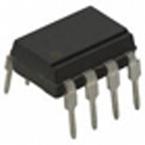
Part Datasheet Search > Amplifiers,Buffers > ADI > AD844AN Datasheet PDF
AD844AN Datasheet PDF - ADI
| Manufacturer: | ADI |
| Category: | Amplifiers,Buffers |
| Case Package: | PDIP-8 |
| Description: | IC OPAMP CF 60MHz 80mA 8DIP |
| Documentation: | AD844AN Datasheet (20 Pages)Package Outline Dimension on19 Page Part Numbering System on20 Page AD844AN Application Note (8 Pages) |
| Pictures: |
AD844AN Datasheet PDF
ADatasheet has not yet included the datasheet for AD844AN
If necessary, please send a supplementary document request to the administrator

AD844AN Datasheet PDF (20 Pages)
AD844AN Specifications
| TYPE | DESCRIPTION |
|---|---|
| Mounting Style | Through Hole |
| Number of Pins | 8 Pin |
| Case/Package | PDIP-8 |
| Supply Current | 6.5 mA |
| Number of Circuits | 1 Circuit |
| Number of Channels | 1 Channel |
| Power Dissipation | 1.1 W |
| Common Mode Rejection Ratio | 100 dB |
| Input Capacitance | 2.00 pF |
| Slew Rate | 2.00 kV/μs |
| Gain Bandwidth Product | 60 MHz |
| Input Impedance | 10.0 MΩ |
| Input Offset Voltage | 50 µV |
| Input Bias Current | 200 pA |
| Operating Temperature (Max) | 85 ℃ |
| Operating Temperature (Min) | -40 ℃ |
| 3dB Bandwidth | 60 MHz |
| Power Dissipation (Max) | 1100 mW |
| Minimum CMRR Range | 95dB ~ 105dB |
AD844AN Size & Package
| TYPE | DESCRIPTION |
|---|---|
| Product Lifecycle Status | Active |
| Packaging | Tube |
| Size-Length | 9.27 mm |
| Size-Width | 7.24 mm |
| Size-Height | 3.43 mm |
| Operating Temperature | -40℃ ~ 85℃ |
AD844AN Environmental
AD844AN Function Overview
Product Details
●The AD844 is a high speed monolithic operational amplifier fabricated using the Analog Devices, Inc., junction isolated complementary bipolar (CB) process. It combines high bandwidth and very fast large signal response with excellent dc performance. Although optimized for use in current-to-voltage applications and as an inverting mode amplifier, it is also suitable for use in many noninverting applications.
●The AD844 can be used in place of traditional op amps, but its current feedback architecture results in much better ac performance, high linearity, and an exceptionally clean pulse response.
●This type of op amp provides a closed-loop bandwidth that is determined primarily by the feedback resistor and is almost independent of the closed-loop gain. The AD844 is free from the slew rate limitations inherent in traditional op amps and other current-feedback op amps. Peak output rate of change can be over 2000 V/μs for a full 20 V output step. Settling time is typically 100 ns to 0.1%, and essentially independent of gain. The AD844 can drive 50 Ω loads to ±2.5 V with low distortion and is short-circuit protected to 80 mA.
●The AD844 is available in four performance grades and three package options. In the 16-lead SOIC (RW) package, the AD844J is specified for the commercial temperature range of 0°C to 70°C.
●The AD844A and AD844B are specified for the industrial temperature range of −40°C to +85°C and are available in the CERDIP (Q) package. The AD844A is also available in an 8-lead PDIP (N). The AD844S is specified over the military temperature range of −55°C to +125°C. It is available in the 8-lead CERDIP (Q) package. A and S grade chips and devices processed to MIL-STD-883B, Rev. C are also available.
●Product Highlights
● 1. The AD844 is a versatile, low cost component providing an excellent combination of ac and dc performance.
● 2. It is essentially free from slew rate limitations. Rise and fall times are essentially independent of output level.
● 3. The AD844 can be operated from ±4.5 V to ±18 V power supplies and is capable of driving loads down to 50 Ω, as well as driving very large capacitive loads using an external network.
● 4. The offset voltage and input bias currents of the AD844 are laser trimmed to minimize dc errors; VOS drift is typically 1 μV/°C and bias current drift is typically 9 nA/°C.
● 5. The AD844 exhibits excellent differential gain and differential phase characteristics, making it suitable for a variety of video applications with bandwidths up to 60 MHz.
● 6. The AD844 combines low distortion, low noise, and low drift with wide bandwidth, making it outstanding as an input amplifier for flash analog-to-digital converters (ADCs).
●Applications
● Flash ADC input amplifiers
● High speed current DAC interfaces
● Video buffers and cable drivers
● Pulse amplifiers
●### Features and Benefits
● Wide bandwidth
● 60 MHz at gain of −1
● 33 MHz at gain of −10
● Slew rate: 2000 V/μs
● 20 MHz full power bandwidth, 20 V p-p, RL = 500 Ω
● Fast settling: 100 ns to 0.1% (10 V step)
● Differential gain error: 0.03% at 4.4 MHz
● Differential phase error: 0.16° at 4.4 MHz
● Low offset voltage: 150 μV maximum (B Grade)
● Low quiescent current: 6.5 mA
● Available in tape and reel in accordance with EIA-481-A standard
show more
AD844AN Documents
AD844 Documents
ADI
ANALOG DEVICES AD844ANZ Operational Amplifier, Single, 1 Amplifier, 60MHz, 2000V/µs, ± 4.5V to ± 18V, DIP, 8Pins
ADI
ANALOG DEVICES AD844JRZ-16 Operational Amplifier, Single, 1 Amplifier, 60MHz, 2000V/µs, ± 4.5V to ± 18V, SOIC, 16Pins
ADI
ANALOG DEVICES AD844BQ Operational Amplifier, Single, 1 Amplifier, 60MHz, 2000V/µs, ± 4.5V to ± 18V, DIP, 8Pins
ADI
18V; 1.5W; 60MHz, 1.1W; 2000V/mS monolithic Op Amp. For flash ADC input amplifiers, high-speed current DAC interfaces
Part Datasheet PDF Search
Example: STM32F103
72,405,303 Parts Datasheet PDF, Update more than 5,000 PDF files ervery day.

