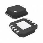
Part Datasheet Search > Analog Switches > ADI > ADG902BCP-500RL7 Datasheet PDF > ADG902BCP-500RL7 Datasheet Pages 1/16
ADG902BCP-500RL7 Datasheet - ADI
| Manufacturer: | ADI |
| Category: | Analog Switches |
| Case Package: | LFCSP |
| Description: | RF Switch SPST 0MHz to 2.5GHz 34dB 8Pin LFCSP EP T/R |
| Pictures: |
ADG902BCP-500RL7Datasheet PDF
Page:
of 16 Go
If the format of the manual is confusing, please download and read the original PDF file.

Wideband, 40 dB Isolation at 1 GHz, CMOS
1.65 V to 2.75 V, SPST Switches
ADG901/ADG902
Rev. B
Information furnished by Analog Devices is believed to be accurate and reliable. However, no
responsibility is assumed by Analog Devices for its use, nor for any infringements of patents or other
rights of third parties that may result from its use. Specifications subject to change without notice. No
license is granted by implication or otherwise under any patent or patent rights of Analog Devices.
Trademarks and registered trademarks are the property of their respective owners.
One Technology Way, P.O. Box 9106, Norwood, MA 02062-9106, U.S.A.
Tel: 781.329.4700 www.analog.com
Fax: 781.461.3113 © 2005 Analog Devices, Inc. All rights reserved.
FEATURES
Wideband switch: −3 dB @ 4.5 GHz
ADG901—absorptive switch
ADG902—reflective switch
High off isolation: 40 dB @ 1 GHz
Low insertion loss: 0.8 dB @1 GHz
Single 1.65 V to 2.75 V power supply
CMOS/LVTTL control logic
8-lead MSOP and tiny 3 mm × 3 mm LFCSP packages
Low power consumption (<1 μA)
APPLICATIONS
Wireless communications
General purpose RF switching
Dual-band applications
High speed filter selection
Digital transceiver front end switch
IF switching
Tuner modules
Antenna diversity switching list
FUNCTIONAL BLOCK DIAGRAM
ADG901
RF2RF1
CTRL
50Ω50Ω
ADG902
RF2RF1
CTRL
03336-001
Figure 1.
GENERAL DESCRIPTION
The ADG901/ADG902 are wideband switches that use a CMOS
process to provide high isolation and low insertion loss to
1 GHz. The ADG901 is an absorptive (matched) switch with
50 Ω terminated shunt legs, while the ADG902 is a reflective
switch. These devices are designed such that the isolation is
high over the dc to 1 GHz frequency range. They have on-board
CMOS control logic, thus eliminating the need for external
controlling circuitry. The control inputs are both CMOS and
LVTTL compatible. The low power consumption of these
CMOS devices makes them ideally suited to wireless
applications and general-purpose high frequency switching.
PRODUCT HIGHLIGHTS
1. −40 dB Off Isolation @ 1 GHz
2. 0.8 dB Insertion Loss @ 1 GHz
3. Tiny 8-Lead MSOP/LFCSP Packages
0
–100
–90
–80
–70
–60
–50
–40
–30
–20
–10
10k 100k 100M1M 10M 1G
10G
03336-002
FREQUENCY (Hz)
ISOLATION (dB)
V
DD
= 2.5V
V
DD
= 1.8V
T
A
= 25°C
Figure 2. Off Isolation vs. Frequency
–3.0
–2.8
–2.2
–1.6
–1.2
–3.0
–2.6
–2.4
–2.0
–1.8
–1.4
–1.0
–0.8
10k 100k 100M1M 10M 1G
10G
03336-003
FREQUENCY (Hz)
INSERTION LOSS (dB)
–0.6
–0.4
V
DD
= 2.5V
T
A
= 25°C
Figure 3. Insertion Loss vs. Frequency
Part Datasheet PDF Search
72,405,303 Parts Datasheet PDF, Update more than 5,000 PDF files ervery day.

