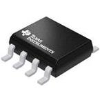
The UCC27212A-Q1 device driver is based on the popular UCC27211 MOSFET drivers. In addition, UCC27212A-Q1 offers extended operating range all the way down to 5 V which helps lower power losses.
●The peak output pullup and pulldown current is 4-A source and 4-A sink, and pullup and pulldown resistance is 0.9 Ω. This allows for the ability to drive large power MOSFETs with minimized switching losses during the transition through the Miller Plateau of the MOSFET.
●The input structure can directly handle –10 V, which increases robustness and also allows direct interface to gate-drive transformers without using rectification diodes. The inputs are also independent of supply voltage and have a 20-V maximum rating.
●The switching node of the UCC27212A-Q1 (HS pin) can handle –18-V maximum, which allows the high-side channel to be protected from inherent negative voltages caused by parasitic inductance and stray capacitance. The UCC27212A-Q1 has increased hysteresis that allows for interface to analog or digital PWM controllers with enhanced noise immunity.
●The low-side and high-side gate drivers are independently controlled and matched to 4 ns between the turn on and turn off of each other.
●An on-chip 100-V rated bootstrap diode eliminates the external discrete diodes. Undervoltage lockout is provided for both the high-side and the low-side drivers which provides symmetric turn on and turn off behavior and forces the outputs low if the drive voltage is below the specified threshold.


