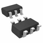
| TYPE | DESCRIPTION |
|---|
| Mounting Style | Surface Mount |
| Number of Pins | 6 Pin |
| Current Rating | 680 mA |
| Case/Package | TSOT-23-6 |
| Number of Positions | 6 Position |
| Drain to Source Resistance (on) (Rds) | 0.33 Ω |
| Polarity | N-Channel, P-Channel |
| Power Dissipation | 900 mW |
| Threshold Voltage | 800 mV |
| Input Capacitance | 63.0 pF |
| Gate Charge | 1.10 nC |
| Drain to Source Voltage (Vds) | 25 V |
| Breakdown Voltage (Drain to Source) | ±25.0 V |
| Breakdown Voltage (Gate to Source) | ±8.00 V |
| Continuous Drain Current (Ids) | 680 mA, 460 mA |
| Rise Time | 9.00 ns |
| Input Capacitance (Ciss) | 50pF @10V(Vds) |
| Input Power (Max) | 700 mW |
| Operating Temperature (Max) | 150 ℃ |
| Operating Temperature (Min) | -55 ℃ |
| Power Dissipation (Max) | 0.9 W |
| TYPE | DESCRIPTION |
|---|
| Product Lifecycle Status | Active |
| Packaging | Tape & Reel (TR) |
| Size-Length | 3 mm |
| Size-Width | 1.7 mm |
| Size-Height | 1 mm |
| Operating Temperature | -55℃ ~ 150℃ |
The FDC6321C is a dual N/P-channel Digital FET with high cell density and DMOS technology. This very high density process is especially tailored to minimize ON-state resistance. The device is an improved design especially for low voltage applications as a replacement for bipolar digital transistors in load switching applications. Since bias resistors are not required, this dual digital FET can replace several digital transistors with difference bias resistors.
● Very low level gate drive requirements allowing direct operation in 3V circuits
● Gate-source Zener for ESD ruggedness
Fairchild
8 Pages / 0.12 MByte
Fairchild
10 Pages / 0.22 MByte
Fairchild
1 Pages / 0.04 MByte
Fairchild
6 Pages / 1.89 MByte
Fairchild
4 Pages / 0.71 MByte
Fairchild
5 Pages / 0.08 MByte
Fairchild
Trans MOSFET N/P-CH 25V 0.68A/0.46A 6Pin SuperSOT T/R
ON Semiconductor
Trans MOSFET N/P-CH 25V 0.68A/0.46A 6Pin SuperSOT T/R
Fairchild
Dual N & P Channel, Digital FET
Part Datasheet PDF Search
72,405,303 Parts Datasheet PDF, Update more than 5,000 PDF files ervery day.


